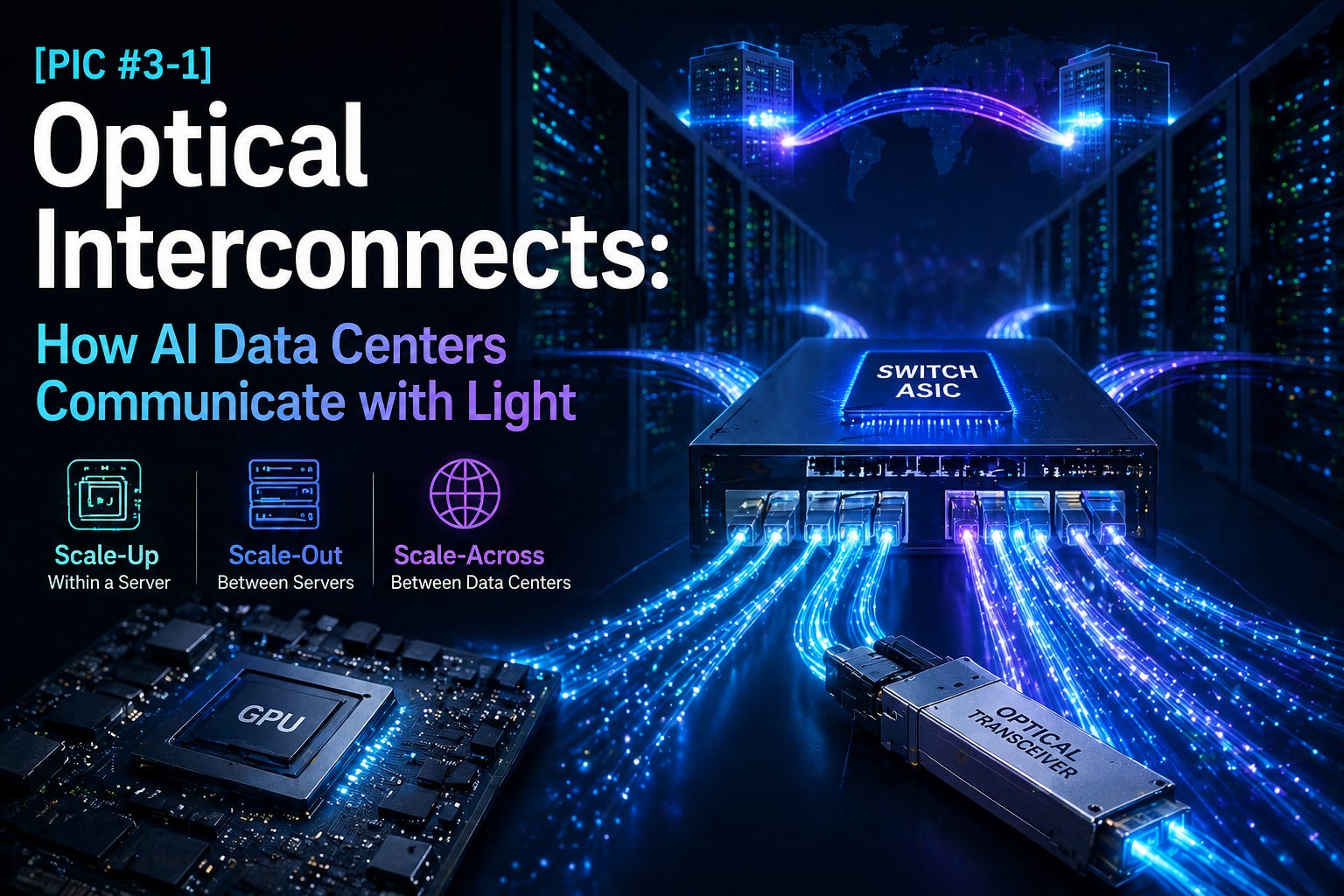
[PIC #3-1] Optical Interconnects: How AI Data Centers Communicate with Light

In our previous posts [PIC #1] and [PIC #2], we explored why light is emerging as a core technology for AI infrastructure. Since the advent of ChatGPT, demand for GPUs has exploded. Training and inferencing AI models now requires thousands, or sometimes tens of thousands, of GPUs working together simultaneously in a single massive cluster.
This is where the problem begins. The more GPUs there are, the more data they need to exchange with each other. In the AI era, the bottleneck is no longer simply “compute performance,” but how quickly chips can communicate with one another.
As explained in [PIC #1], copper-based connections (copper interconnects) are increasingly struggling to meet these demands. As data transfer speeds (bandwidth) increase, copper wires generate more heat, signal loss worsens, and power consumption rises rapidly. These limitations become even more pronounced as transmission distances grow.
The answer is light. Instead of electrical signals over copper traces, data is transmitted as optical signals through optical fiber. Compared to copper, optical fiber offers far lower signal loss, virtually no heat generation, and is especially advantageous for long-distance and high-speed transmission.
But one more problem remains (see [PIC #2]). Most semiconductor chips, including GPUs, memory, and switch ASICs, still operate on electrical signals. If computation relies on electrical signals while data transmission is done with light, a device capable of freely converting between the two is needed. That device is the optical transceiver. A transceiver converts electrical signals into optical signals for transmission, and converts received optical signals back into electrical signals.
This shift is not a future story. It is already rapidly unfolding in the market. According to market research firm TrendForce, global shipments of 800G and above optical transceivers are projected to surge from 24 million units in 2025 to 63 million in 2026, roughly a 2.6× increase [1]. This is a clear signal that the industry is rapidly transitioning from copper to optics.
1. Transceivers: Converting Between Electrical and Optical Signals
An optical transceiver is a portmanteau of transmitter and receiver. Again, it is a device that converts electrical signals into optical signals for transmission, and converts received optical signals back into electrical signals.
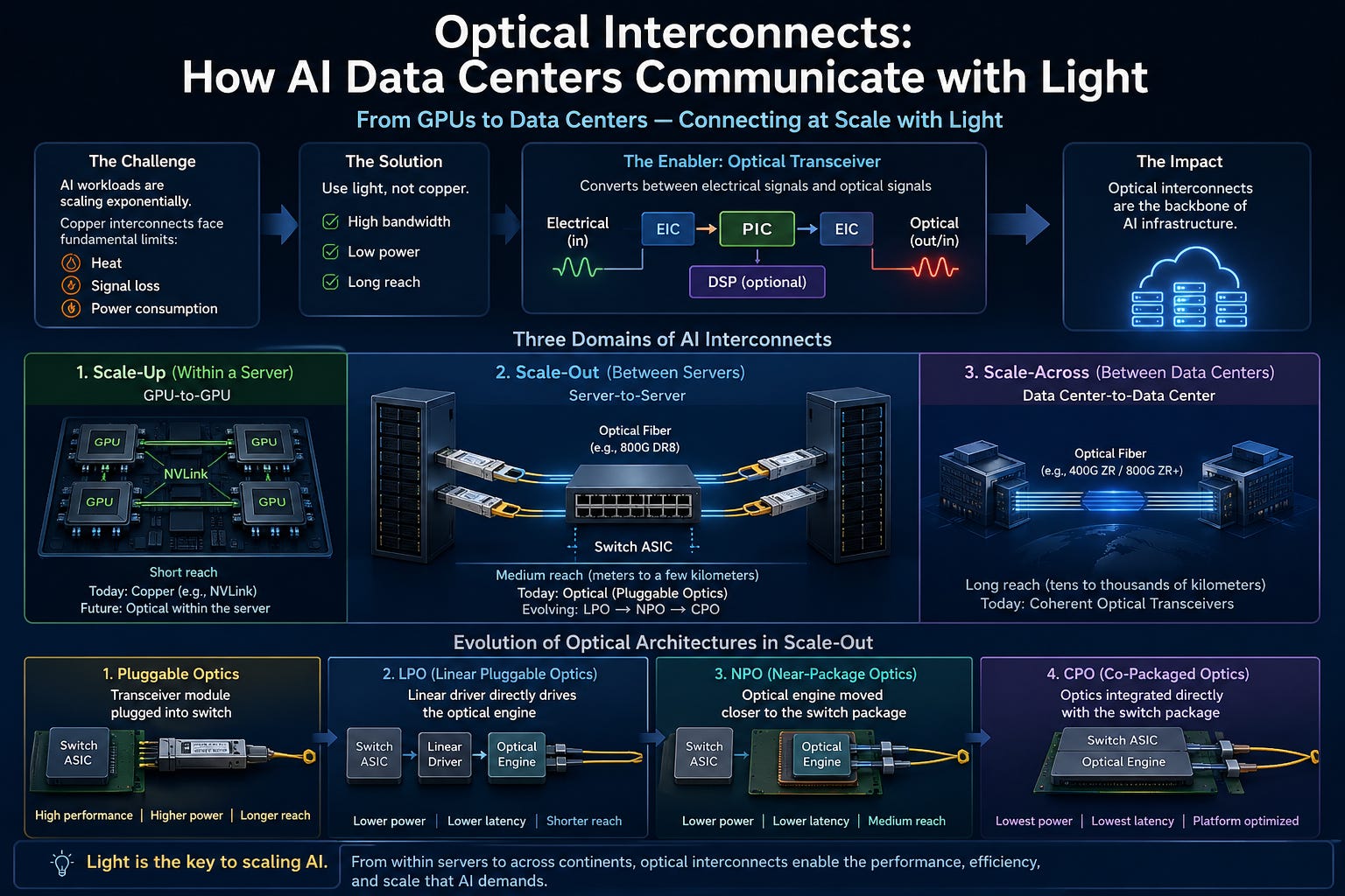
Today’s optical transceivers are generally composed of a PIC (Photonic Integrated Circuit) for optical functions, an EIC (Electrical Integrated Circuit) to drive it, and in some cases a DSP (Digital Signal Processor) responsible for signal correction and recovery. Together with packaging and optical connectors, this assembly is called a transceiver module.
So how are these transceivers actually used in AI data centers? To understand this, we first need to look at how GPUs are interconnected. Today, interconnects can be broadly divided into three domains [2]: scale-up, scale-out, and scale-across. This post will cover scale-up and scale-out first.
Note: PhotonCap covers related topics in greater breadth. I recommend reading alongside [3].
2. Scale-Up: GPU-to-GPU Connections Within a Server

Figure 1. Scale-up: GPU-to-GPU connections within a single GPU server.
Today, a single AI server contains multiple GPUs. These GPUs must divide up a model for parallel computation, or exchange data with each other during parallel operations. Therefore, GPU-to-GPU connection performance inside a server directly impacts overall AI system performance.
Scale-up refers to the shortest-distance connections among the three interconnect categories, specifically, GPU-to-GPU connections within a single server. Currently, this domain is still dominated by copper-based electrical interconnects. A representative example is NVIDIA’s NVLink [4]. Because GPUs within the same server are physically very close to each other, electrical signals alone can still provide sufficiently high bandwidth.
The problem, however, is that AI servers keep growing.
The number of GPUs per server is increasing, the data throughput per GPU is rising, and the traffic that GPUs must exchange with each other is exploding. In other words, even within a server, the burden on copper traces is inevitably growing. As repeatedly emphasized in previous posts, the faster the speed, the more severe the issues of heat, signal loss, and power consumption become with copper.
While scale-up electrical connections are not switching to optical immediately, in the long term, I strongly believe that optical interconnects will make their way into intra-server connections as well.
The company most prominently demonstrating this direction is Ayar Labs. Having received strategic investment from NVIDIA, this company is developing an optical I/O (input/output) chiplet called TeraPHY. The goal is to place optical engines within GPU servers to transition existing NVLink-based electrical connections into optical signals. In March 2026, Ayar Labs raised approximately $500 million in a Series E round with participation from NVIDIA, MediaTek, and others [5]. This is a signal that the industry is taking optical interconnects within servers seriously.
3. Scale-Out: GPU Server-to-Server Connections

Figure 2. Scale-out: GPU server-to-server connections.
In today’s AI data centers, scale-out is the most critical domain for optical interconnects. In general, scale-out refers to longer connection than scale-up, like GPU server-to-GPU server (strictly speaking, the connection is mediated by a switch ASIC, but at this stage, it is sufficient to think of it as server-to-server connection). Compared to the distance between GPUs within a single server, server-to-server distances are relatively long, making the limitations of copper-based electrical signals (i.e., heat, signal loss, and power consumption) very apparent. Moreover, as data transfer speeds increase, copper cables must become thicker, which not only takes up precious physical space but also adds significant weight.
As shown in the figure above, the interconnect between racks of GPU servers is called rack-to-rack interconnect, and the physical distances involved are beyond what copper can reliably handle. Even when GPU servers are relatively close to each other, as the number of servers that need to communicate grows, the distances of data travel continue to increase.
In other words, for relatively long-distance connections such as server-to-server or rack-to-rack, optical interconnects are essential.
However, as the number of servers that need to be connected grows, it is not only the distance that becomes more complex, but also the way they communicate does too. Let’s look more closely at how GPU servers are connected.

Figure 3. Example of direct connections between all GPU servers (illustrative example of a naive approach).
Intuitively, you might think of directly connecting each GPU server with optical fiber. For example, connecting 2 GPU servers requires 1 link. Connecting 4 servers requires 6 links, and 8 servers requires 28 links. What about 5,000 GPU servers?
As the number of servers grows, the number of required links increases exponentially.
The key device that solves this problem is the switch ASIC (Application-Specific Integrated Circuit).
3-1. Switch ASIC: The Center of Traffic
A switch ASIC is like a traffic control center. It receives data coming in from multiple ports, determines which destination each packet should be forwarded to, and routes it along the appropriate path. It enables large-scale many-to-many communication, rather than simple point-to-point connections.
With a switch ASIC, each GPU server no longer needs to be directly connected to every other server. Instead, each server simply needs a connection to the switch ASIC. Even with 1,000 GPU servers, each server only needs a few links to the switch ASIC to communicate with all others.
So how does the actual signal flow?

Figure 4. Example of server–transceiver–switch ASIC–transceiver–server signal flow.
From the GPU server, an optical signal is sent toward the switch ASIC. A transceiver near the switch ASIC converts the optical signal into an electrical signal and delivers it to the switch ASIC. The switch ASIC processes this electrical signal, determines the destination GPU server, and converts it back to an optical signal through another transceiver. That light travels through optical fiber to the destination GPU server’s transceiver, where it is finally read as an electrical signal.
As AI infrastructure scales, raw GPU performance alone is not enough. How quickly GPUs can exchange data with each other determines overall system performance. At the center of that is the scale-out network and the switch ASIC. As optical communication grows, the switch ASIC market is therefore structurally bound to grow with it.
The leading companies in switch ASICs include Broadcom, NVIDIA, and Marvell. A notable recent example is Broadcom’s Tomahawk 6, which supports up to 102.4 Tbps and 512 ports [6].
3-2. Connecting the Switch ASIC and the Optical Transceiver
Now let’s discuss something more important.
As explained above, long-distance data transmission is handled by light, while the switch ASIC handles data routing. However, the switch ASIC is still a semiconductor that processes electrical signals. This means that optical signals arriving through optical fiber must be converted into electrical signals before reaching the switch ASIC, which is the job of the optical transceiver.
After the optical signal is converted into an electrical signal inside the transceiver, it travels along copper traces to the switch ASIC. Yes, copper becomes a problem again: heat, signal loss, and power consumption. The length of this copper segment, which is the distance between the transceiver and the switch ASIC, has a significant impact on scale-out link performance.
Light has solved the long-distance segment, but this last electrical segment remains.
One of the areas where the industry is fiercely competing is precisely here. The key question is: “how close can the switch ASIC and transceiver be placed?” Let’s look at the available approaches.
[1] Pluggable Optics: The Current Standard

Figure 5. Example diagram of pluggable optics.
The current mainstream approach is pluggable optics. As the name implies, the transceiver module is inserted into a slot at the edge of the switch ASIC board. These slots follow standardized form factors, such as QSFP (Quad Small Form-factor Pluggable).
As shown in the figure above, light enters the transceiver module through optical fiber, where the optical signal is converted to an electrical signal. The converted electrical signal then travels along copper traces from the board edge to the switch ASIC.
The greatest advantage of pluggable optics is ease of replacement. If a transceiver fails, you simply unplug the fiber, remove the module, and plug in a new one. Standardization is also well-established, so modules from any manufacturer are interoperable. This is why pluggable optics has been the market standard for so long.
Paradoxically, another advantage is that the laser (light source) inside the transceiver module is relatively far from the switch ASIC. Lasers are temperature-sensitive, and switch ASICs generate substantial heat.
However, as previously discussed, the problem is the copper segment connecting the switch ASIC to the transceiver at the board’s edge. At high speeds, this segment becomes the bottleneck. As we have said repeatedly: as data transfer speeds increase, copper’s heat, signal loss, and power consumption become increasingly problematic.
In summary, pluggable optics is easy to replace and well-standardized, but as data transfer speeds increase, it inevitably hits its limits.
[2] LPO (Linear Pluggable Optics)
The next step gaining attention beyond pluggable optics is LPO (Linear Pluggable Optics).
LPO retains the advantages of conventional pluggable optics while adding new ones.
A typical transceiver module contains two key components: the optical section (lasers, photodetectors, photonic and electronic integrated circuits, etc.) that converts between electrical and optical signals, and the DSP (Digital Signal Processor). The DSP corrects and compensates for signal quality. While the DSP is critically important for signal integrity, it also carries drawbacks: high power consumption, heat generation, cost, and signal processing latency.
LPO removes the DSP from inside the transceiver module and delegates its role to the host system, such as the switch ASIC. The benefits are reduced transceiver power consumption, reduced signal processing latency, and lower cost, while the module remains pluggable and therefore replaceable.
However, the drawbacks are equally clear. Without a DSP inside the transceiver, the incoming optical signal must already be of sufficient quality to require no correction or compensation. Since signal quality generally degrades with distance, LPO is only advantageous for relatively short-distance connections within a data center [7].
Moreover, since LPO does not address the fundamental issue, which is the copper segment between the switch ASIC and the transceiver, the challenges seen in conventional pluggable optics at high speeds remain unresolved.
LPO can be seen as a step toward maximizing the efficiency of pluggable optics before moving to the next stage.
[3] Near-Package Optics (NPO)
 architecture, including ASIC, PIC, remote laser, and various electrical and optical interfaces, culminating in a high-performance motherboard.
AI-generated content may be incorrect.")
Figure 6. Example diagram of NPO (Near-Package Optics). Note that there are various ways to implement NPO, so the figure above represents one example. The key point is that the optical engine exists on the switch ASIC board as an independent module.
NPO (Near-Package Optics) emerged to address the fundamental limitation of pluggable optics and LPO; namely, the long copper segment between the transceiver and the switch ASIC.
For reference, the core part of a transceiver responsible for actual optical-to-electrical signal conversion is commonly called the optical engine, typically consisting of a PIC (Photonic Integrated Circuit) and the EIC (Electronic Integrated Circuit) that drives it.
In NPO, rather than using the entire conventional transceiver module, the discussion centers on simplifying the structure around this core optical engine and placing it close to the switch ASIC. The optical engine is not placed within the exact same package as the switch ASIC, but is maintained as a separate module placed in close proximity.
Since the distance between the switch ASIC and the optical engine is reduced to just a few centimeters, NPO offers significant advantages over pluggable optics and LPO (Linear Package Optics) in terms of heat, power consumption, and bandwidth [7].
Of course, NPO is not the ultimate solution. A few centimeters of copper wire still cannot be ignored at very high speeds.
[4] CPO (Co-Packaged Optics)
 architecture integrating ASICs, photonic integrated circuits, and optical engines on a shared substrate, with electrical connections, lasers, and a motherboard for high-performance applications.
AI-generated content may be incorrect.")
Figure 7. Example diagram of CPO (Co-Packaged Optics). Note that there are various ways to implement CPO, so the figure above represents one example. The key point is that the optical engine is inside the same package as the switch ASIC, making the copper distance between the two extremely short.
CPO (Co-Packaged Optics) takes NPO one step further by placing the optical engine within the same package as the switch ASIC, minimizing the copper distance between them to the absolute minimum.
CPO is not yet fully standardized, and there are various architectures and approaches for implementing it [8, 9]. But the conclusion is the same: “place the switch ASIC and optical engine as close together as possible within the same package.”
This is exactly the same logic as the evolution of memory such as HBM (High Bandwidth Memory) covered in [PIC #1]. Just as HBM was placed right next to the GPU to dramatically reduce the memory-GPU bottleneck, placing the optical engine right next to the ASIC minimizes the bottleneck at the electrical-to-optical signal conversion stage.
But there are many challenges to overcome.
The first is the repair and replacement problem. Pluggable modules can be replaced on the spot if they fail. With CPO, however, since the optical engine and switch ASIC share the same package, repairs can be far more complex when a failure occurs.
The second is the laser heat problem. Switch ASICs are major heat sources, and lasers are extremely sensitive to temperature (even small changes can affect performance). Placing a laser right next to a hot ASIC therefore raises serious reliability concerns. For this reason, CPO often adopts an ELS (External Light Source) approach, where the laser is separated into a module outside the package. Lumentum is developing a standardized ELS form factor called ELSFP [10], and Coherent is supplying 400 mW CW (continuous wave) lasers as a light source for CPO [11].
The third is the yield problem. When the ASIC die and optical engine are packaged together, if either one is defective, the entire assembly may be scrapped. This makes KGD (Known Good Die) testing — fully validating optical dies before packaging — an essential requirement.
The fourth is the fiber attachment problem. In pluggable optics, you simply plug an optical fiber connector into the transceiver. With CPO, optical fibers must be directly attached to the package level, requiring extremely high alignment precision and manufacturing throughput.
The fifth is insufficient standardization. Pluggable optics benefits from standards like QSFP and OSFP, ensuring interoperability regardless of manufacturer. CPO requires much closer collaboration between ASIC and optical vendors, and industry standards have not yet matured. Standardization efforts are being discussed within the OIF (Optical Internetworking Forum), but remain in early stages.
Nevertheless, CPO is becoming a reality. Without placing the optical engine and switch ASIC closer together, it will be very difficult to resolve the power and bandwidth challenges facing data center networks.
The market is already responding to this. Broadcom’s Tomahawk 6 was announced as a CPO switch [6]. At Meta’s test environment, a Broadcom CPO link was reported to have operated for a cumulative one million hours without a single link flap [12].
The next step beyond CPO is monolithic integration — going beyond co-packaging the optical engine in the same package, this approach aims to directly integrate electronic circuitry (including the switch ASIC) with optical circuitry at the chip level. While still in its early stages, it is frequently cited as the ultimate direction for optical interconnects.
Conclusion
At the heart of AI data centers is the interconnect between devices, which determines data transfer speed. Copper-based data transmission is approaching its limits, and to address this, optical signal-based transmission is essential.
Interconnects can be roughly divided into three categories (scale-up, scale-out, and scale-across) based on transmission distance (though this is a simplification). This post covered scale-up and scale-out.
Scale-up refers to GPU-to-GPU connections within a single GPU server. Because of the relatively short distances involved, copper-based electrical interconnects are still used. However, as transmission speeds and distances within servers continue to increase, copper’s fundamental problems—heat, signal loss, and power consumption—will become increasingly severe. Efforts to replace this domain with optical signals are therefore actively underway.
Scale-out refers to GPU server-to-server connections. Because of the relatively long distances involved, the limitations of copper are clear and optical signals are essential. This is why scale-out is the most actively researched and developed domain in optical interconnects. The key lies in the switch ASIC, which routes signals between GPU servers, and the transceiver modules.
Since the switch ASIC operates on electrical signals, a transceiver module near the ASIC converts optical signals to electrical signals and delivers them. However, the connection between the switch ASIC and the transceiver module runs through copper, and this segment acts as a bottleneck. At high speeds, copper’s heat, signal loss, and power consumption are problematic.
As a result, significant effort is being directed toward reducing the physical distance between the switch ASIC and the transceiver module (or optical engine). In this post, we covered four approaches: pluggable optics, LPO (Linear Pluggable Optics), NPO (Near-Package Optics), and CPO (Co-Packaged Optics).
The next post will continue from here and discuss scale-across.
References
[1] TrendForce, “AI Data Centers Ignite a Laser Shortage Wave,” December 8, 2025. https://www.trendforce.com/presscenter/news/20251208-12823.html
[2] NVIDIA, “Scaling Out and Across: Networking Innovations for Giga-Scale AI Systems,” GTC San Jose, March 2026. https://www.nvidia.com/ko-kr/on-demand/session/gtc26-s81561/
[3] Photon Capitol, “NVIDIA’s $2B Marvell Bet and Celestial AI’s “25x Bandwidth” Claim: What’s the Denominator?” Substack Post.

[4] NVIDIA, “NVIDIA NVLink and NVLink Switch.” https://www.nvidia.com/en-us/data-center/nvlink/
[5] T. Mann, “Ayar Labs raises $500M to mass-produce CPO chiplets,” The Register, March 3, 2026. https://www.theregister.com/2026/03/03/ayar_labs_500m/
[6] Broadcom, “Tomahawk 6 / BCM78910 Series”. https://www.broadcom.com/products/ethernet-connectivity/switching/strataxgs/bcm78910-series
[7] NADDOD, “Optical Interconnect Technology Analysis: LPO, NPO, CPO,” November 12, 2025. https://www.naddod.com/blog/optical-interconnect-technology-analysis-lpo-npo-cpo
[8] Semianalysis, “Co-Packaged Optics (CPO) Book – Scaling with Light for the Next Wave of Interconnect,” January 1, 2026.

[9] IDTechEx, “Co-Packaged Optics (CPO): Evaluating Different Packaging Technologies,” August 22, 2024. https://www.idtechex.com/ko/research-article/co-packaged-optics-cpo-evaluating-different-packaging-technologies/31608
[10] BusinessWire, “Lumentum Demonstrates Industry-Leading Technologies and Products for Scale-Out, Scale-Up and Scale-Across AI Infrastructure at OFC 2026,” March 17, 2026. https://www.businesswire.com/news/home/20260317080634/en/Lumentum-Demonstrates-Industry-Leading-Technologies-and-Products-for-Scale-Out-Scale-Up-and-Scale-Across-AI-Infrastructure-at-OFC-2026
[11] Coherent Corp., “Coherent Demonstrates Multiple Technologies for Co-packaged Optics (CPO) at OFC 2026,” March 2026. https://www.coherent.com/news/press-releases/coherent-co-packaged-optics-cpo-technologies-ofc-2026
[12] Broadcom, “Broadcom Showcases Industry-Leading Quality and Reliability of Co-Packaged Optics,” October 1, 2025. https://investors.broadcom.com/news-releases/news-release-details/broadcom-showcases-industry-leading-quality-and-reliability-co?utm_source=chatgpt.com